
Direct-bandgap platform
InP and compatible III–V alloys underpin active optoelectronic structures. This makes the platform relevant to light generation and detection, unlike using silicon alone as a conventional light-emitting material.
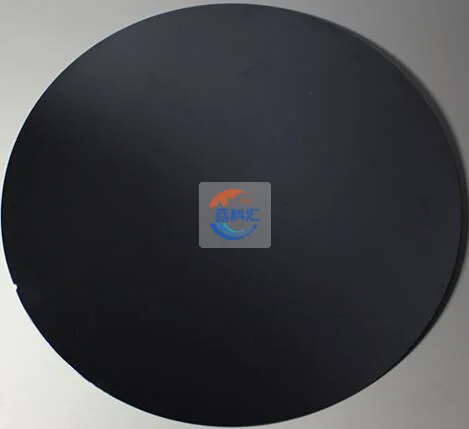
Indium phosphide substrates for optical communication, integrated photonics and high-frequency electronics. Start with the material. Build toward your next device.
Request a specification review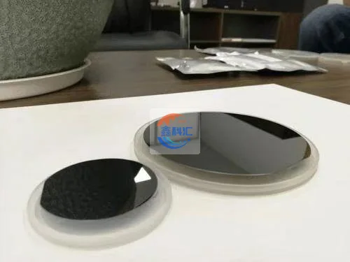
Crystal quality. Surface finish. Electrical properties. The right specification connects them.
Explore material parametersInP single crystals are a substrate platform, not a finished optical device. Their value emerges through the epitaxial layers, fabrication process and architecture built on top.
InP substrates support epitaxial compound-semiconductor structures used in telecom lasers and photodetectors. Devices based on InP-compatible material systems can operate around the important 1.3 and 1.55 micrometre fibre-optic bands; the emission wavelength is set by the active layer, not the bare substrate.
Laser wavelength, detector response, bandwidth and efficiency belong to the completed device. They must not be interpreted as guaranteed performance of an unprocessed InP wafer.
Choose an indium phosphide substrate for its role in your device stack, then qualify the electrical, crystallographic and surface characteristics that matter to that process.
InP and compatible III–V alloys underpin active optoelectronic structures. This makes the platform relevant to light generation and detection, unlike using silicon alone as a conventional light-emitting material.
Lattice-matched InGaAs and InGaAsP material systems are central to many InP-based devices. Layer composition and strain must be designed for the substrate and target wavelength.
Conductive and semi-insulating InP serve different device architectures. Carrier concentration, mobility and resistivity should be part of an agreed acceptance specification.
Polishing, cleanliness, orientation and near-surface damage affect subsequent processing. Wafer inspection and epitaxy trials establish fitness for your particular process.
Separate intrinsic material properties from purchase specifications. The fields below help you define an InP wafer inquiry without assuming an unverified stock grade.
| Property | Reference / description | Engineering relevance |
|---|---|---|
| Material / formula | Indium phosphide / InP | Binary III–V compound semiconductor |
| Crystal structure | Cubic zinc blende | Orientation and cleavage behaviour |
| Bandgap character | Direct | Optoelectronic material-system selection |
| Common substrate orientation | (100); offcut to be specified | Epitaxial growth and device processing |
| Electrical families | Conductive n-type / semi-insulating | Different conduction and isolation requirements |
| Associated epitaxial systems | InGaAs / InGaAsP, composition dependent | Lattice matching and active-layer engineering |
| Specification field | What to include in your inquiry | Confirmation basis |
|---|---|---|
| InP diameter / crystal format | Required diameter in mm; full wafer or diced piece | Size, tolerance and available format |
| InP wafer thickness | Target thickness in µm and tolerance | Wafer handling and process compatibility |
| InP orientation / offcut | Plane, offcut angle and direction | Crystallographic measurement |
| InP doping / electrical type | n-type or semi-insulating; preferred dopant | Confirmed grade and lot data |
| InP carrier concentration | Acceptance range in cm⁻³ | Agreed measurement method |
| InP resistivity / mobility | Ω·cm / cm²·V⁻¹·s⁻¹; test temperature | Agreed electrical characterization |
| InP dislocation density | Maximum EPD in cm⁻²; inspection area | Etch and counting method to be agreed |
| InP surface finish | SSP or DSP; front/back treatment | Polishing and surface acceptance |
| InP surface roughness | Ra or RMS in nm; scan area | AFM method and sampling plan |
| InP TTV / bow / warp | Separate limits in µm | Measurement conditions and wafer support |
| InP edge / identification | Flat or notch, bevel, ID marking | Handling equipment compatibility |
| InP packaging / documentation | Quantity, packaging, inspection report, CoA request | Written quotation and delivery agreement |
No assumed catalogue tolerances. The supplied company brochures identify InP as a product, but do not provide a legible, confirmed InP specification sheet. Numerical wafer limits, diameter availability, price range, stock status and lead time are therefore subject to quotation.
Build your inquiryTell us your epitaxial system, device application and process constraints. Distinguish conductive from semi-insulating substrate needs.
Review geometry, orientation, electrical properties, surface quality, inspection methods and packaging in writing.
Request a quotation with the available grade, quantity, lead time, inspection documents and shipping terms.
Use an evaluation lot to assess handling, cleaning and epitaxy before approving a material for repeat procurement.
shanghai xinkehui new materails co.,ltd is a technology-focused company working in the production, processing and sales of semiconductor substrates and optical crystal materials.
Our public company literature includes InP, silicon, silicon carbide, sapphire, optical windows and other crystal materials. We bring application-led discussion and specification review to customers in semiconductor, optoelectronic and optical communication fields.
For this InP project, speak directly with our Shanghai team about your material requirements and the documentation you need for qualification.
Connect with our materials teamCustomer-centered.
Quality-focused.
Material acceptance criteria and supply commitments are confirmed for the actual order.
Share your drawing, process requirements and evaluation goals with our Shanghai team.
Practical answers for research, device development and procurement.
Have a different question?InP is single-crystalline indium phosphide, a III–V compound semiconductor. A wafer sliced and finished from the crystal can act as a substrate for epitaxial layers and device fabrication.
InP substrates are used in material systems for optical communication lasers, photodetectors, photonic integrated circuits and high-frequency electronic devices. The final device and epitaxial stack determine performance.
No. The wavelength of an InP-based laser is engineered through its active-layer composition and device design. A bare InP substrate must not be described as a finished 1.55 µm laser.
n-type InP is conductive and provides electron carriers. Semi-insulating InP has high resistivity and is used where electrical isolation is important. Confirm doping, carrier concentration and resistivity for your architecture.
(100) is a common InP substrate orientation. Your epitaxial process may require a specific offcut angle and direction. Specify these explicitly for your InP order rather than assuming a standard orientation.
SSP means single-side polished; DSP means double-side polished. InP finish selection depends on front-surface processing, backside requirements, handling and measurement needs. Both InP surfaces should be specified in the inquiry.
Not on this page. Send the required InP diameter, thickness and tolerances to Xinkehui. Available InP formats and dimensions must be confirmed in the quotation before ordering.
TTV describes thickness variation, while bow and warp describe InP wafer shape under defined measurement conditions. They can affect handling, chucking, lithography and processing. Specify each InP limit separately.
Request the agreed InP lot identification, dimensions, electrical data and crystal or surface inspection results relevant to your process. Ask which InP tests and certificates can be supplied before placing an order.
Keep InP wafers in suitable protective packaging and handle them with trained personnel and cleanroom-compatible tools. Avoid edge impacts, dust and uncontrolled chemicals. Obtain the InP supplier safety data sheet before cutting, grinding or chemical processing.
InP is a substrate for suitable InGaAs compositions and related heterostructures. Lattice matching depends on composition; your epitaxial design and qualification results must establish compatibility.
These are quote-dependent and not confirmed online. InP pricing depends on grade, dimensions, electrical and surface requirements, quantity, inspection and delivery terms. Request a dated InP quotation for current availability.
Include the device application, InP diameter, thickness, orientation and offcut, electrical type, doping requirements, surface finish, defect limits, quantity, delivery location and required documents.
Share your InP single crystal or wafer requirements. We will review the specification and confirm the scope of supply.
[email protected] +86 132 6287 9223Chat on WhatsAppRoom 1805, Building 1, Wanda Mall
1079 Dianshanhu Avenue, Qingpu District
Shanghai, China
Price range: by quotation · Stock: confirmation required